CIES Consortium
Industry-Academic Collaboration
Spintronics LSI Technology
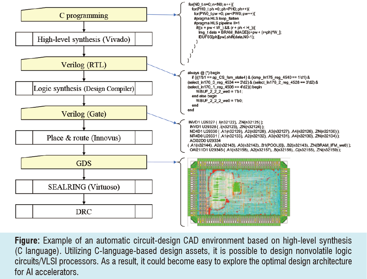
R&D of technologies to automatically design environments for low-energy consumption and highly functional VLSI processors based on non-volatile memory
-
 Research Director
Prof.
Takahiro Hanyu -
 Research Director
Associate Prof.
Daisuke Suzuki
To overcome a power-wall problem in 4x-nm CMOS era and beyond, our R&D project aims to develop nonvolatile (NV)-device-based logic-circuit Intellectual Properties (IPs) and its automatic design environment. The actual development items are as follows:
- Development of a CAD environment for NV-FPGAs
FPGAs (Field-Programmable Gate Array) is a attractive hardware platform for various applications. We have been establishing the environment by combining an open-source CAD tool, called Verilog-to-Routing (VTR), with nonvolatile logic-circuit IPs. - Development of a NV-based circuit IPs
We have also been developing logic circuit IPs for realizing a further energy-efficient/highly functional NV-FPGA. - Applications to AI accelerators
As an effective application, we have been developing NV-FPGA-based energy-efficient AI accelerator.
It is expected that the NV-FPGA is utilized in a wide variety of applications such as IoT and mobile devices.